 首页
首页 400-620-6333
切换导航

搜索


基本描述
| 规格或纯度 | 氨型 |
|---|---|
| 英文名称 | Electroless nickel plating solution |
| 产品介绍 |
Description Improved standard electroless nickel plating composition specific for making ohmic contacts to silicon and other semiconductor materials.Advantages:Stable, ready to usePlates uniformly on p- and n- type siliconOffers excellent adhesion and solderabilityPlates on silicon, germanium, gallium arsenideProduces quality electrical contacts on p- and n- type siliconAn improved electroless nickel plating solution (Brenner type) formulated for semiconductor use. Specifically, it is designed to deposit nickel uniformly and at equal plating rates on both p- and n- type silicon. The composition of this product is based upon ions of nickel complexes and hypophosphite with stabilizers. Only high purity chemicals are used. The plating solution is a stable product ready to use without the need for additions or mixing. Transene Electroless Nickel Plating Ammonia Type operates under conditions of a catalytic oxidation-reduction reaction between nickelous and hypophosphite ions. The chemical reaction is essentially a two-step process occurring simultaneously.H2PO2-+ H2O --> H2PO3 -+ 2H++ 2e-(1)Ni2++ 2e---> Ni (2)Nickel is deposited containing about 1% phosphide which improves the physical properties of the metalization.The plating solution has an optimized standard electrode potential of 0.44 volts. The electrode characteristics help to regulate the difference in electronegativity between p- and n- type silicon relative to the potential of the nickel complex ions. Thus the rate of deposition of nickel on p- and n- silicon is equalized. The deposition on p- and n- type silicon is 2,000 ?/minute at 90 °C.Silicon surfaces must be clean and etched in Buffer-HF or HF solution to remove oxide, rinsed and stored in alcohol. On polished silicon wafers, plate 1000-2000 A of electroless nickel; greater thickness on lapped silicon surfaces. The deposited nickel can be sintered into silicon at 500 °C to 750 °C to promote adhesion and ohmic contact. A second nickel deposit is generally required. Description Improved standard electroless nickel plating composition specific for making ohmic contacts to silicon and other semiconductor materials.Advantages:Stable, ready to usePlates uniformly on p- and n- type siliconOffers excellent adhesion and solderabilityPlates on silicon, germanium, gallium arsenideProduces quality electrical contacts on p- and n- type siliconAn improved electroless nickel plating solution (Brenner type) formulated for semiconductor use. Specifically, it is designed to deposit nickel uniformly and at equal plating rates on both p- and n- type silicon. The composition of this product is based upon ions of nickel complexes and hypophosphite with stabilizers. Only high purity chemicals are used. The plating solution is a stable product ready to use without the need for additions or mixing. Transene Electroless Nickel Plating Ammonia Type operates under conditions of a catalytic oxidation-reduction reaction between nickelous and hypophosphite ions. The chemical reaction is essentially a two-step process occurring simultaneously.H2PO2-+ H2O --> H2PO3 -+ 2H++ 2e-(1)Ni2++ 2e---> Ni (2)Nickel is deposited containing about 1% phosphide which improves the physical properties of the metalization.The plating solution has an optimized standard electrode potential of 0.44 volts. The electrode characteristics help to regulate the difference in electronegativity between p- and n- type silicon relative to the potential of the nickel complex ions. Thus the rate of deposition of nickel on p- and n- silicon is equalized. The deposition on p- and n- type silicon is 2,000 ?/minute at 90 °C.Silicon surfaces must be clean and etched in Buffer-HF or HF solution to remove oxide, rinsed and stored in alcohol. On polished silicon wafers, plate 1000-2000 A of electroless nickel; greater thickness on lapped silicon surfaces. The deposited nickel can be sintered into silicon at 500 °C to 750 °C to promote adhesion and ohmic contact. A second nickel deposit is generally required. |
产品问答
产品问答
上海阿拉丁生化科技股份有限公司
? 2016 ALADDIN-E.COM . 版权所有,未经授权禁止拷贝本站资料,如有违反,将追究法律责任


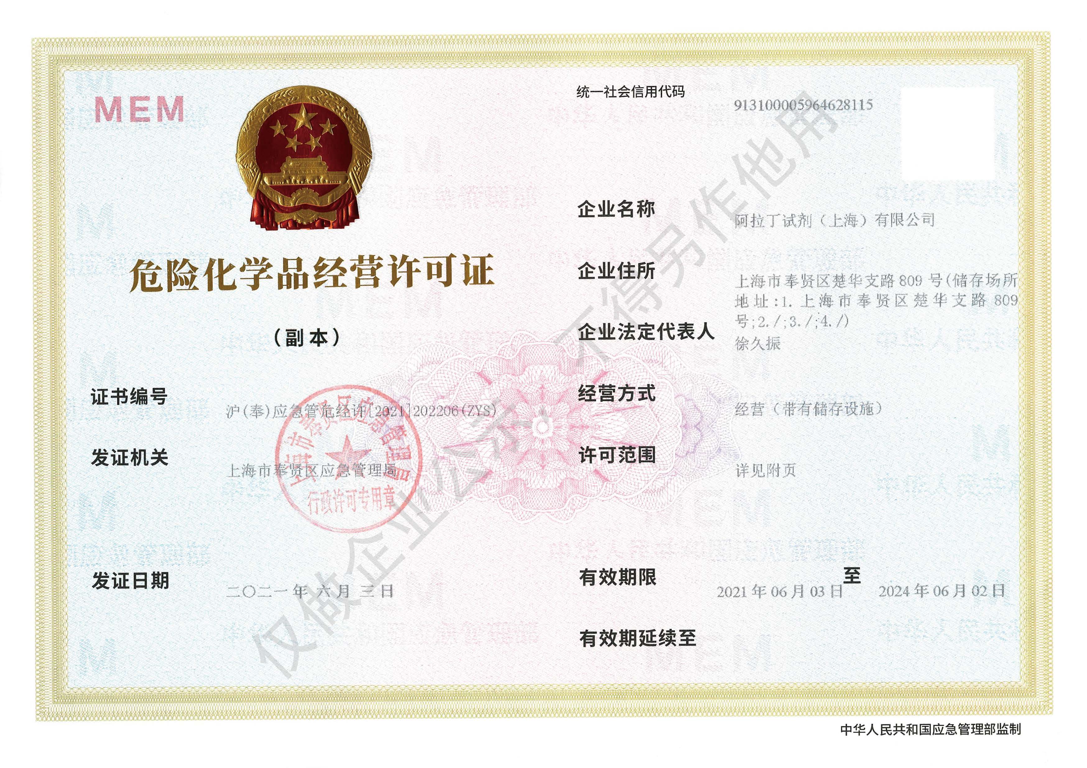 危险品化学品经营许可证(带存储)