 首页
首页 400-620-6333
Inorganic Interface Layer Inks for Organic Electronic Applications
INTRODUCTION
As light undergoes conversion into electrical charges in Organic Photovoltaics (OPV) or electricity transforms into light in Organic Light-Emitting Diodes (OLED), the interface layers in both systems play a pivotal role in securing optimal device efficiency. To elaborate, interface layers selectively facilitating the passage of charge carriers are vital. Hole-selective interface layers, for instance, ensure the efficient transportation of holes from the active layer to the electrode by impeding the movement of electrons. Conversely, electron-selective interface layers ensure the smooth transport of electrons while hindering the migration of holes. Advanced solution-processable materials at the forefront of this technology include PEDOT:PSS, serving as a hole-selective organic substance, and sol-gel deposited zinc oxide (ZnO), employed as an electron-selective material.
?
Polymers such as PEDOT:PSS face significant challenges, with acidity being a primary concern that adversely affects device stability. Additionally, their organic nature, characterized by relatively modest chemical stability, presents another drawback. As for sol-gel ZnO, limitations include a brief shelf life, a lack of reproducibility, and the requirement for elevated annealing temperatures. Consequently, there exists a pressing necessity to substitute these materials with alternatives that are suitable for industrial applications.
?
A range of inorganic charge-selective inks enable cost-effective solution-processed OPV or OLED fabrication on flexible or rigid substrates using printing techniques such as slit dye coating or spin coating. The next generation of these inks is currently being optimized for inkjet or screen printing. Zinc oxide nanoparticle inks and Tungsten oxide (WO3-x) nanoparticle inks are nanoparticle-based printing inks that allow processing temperatures of 80°C (Table 1).
|
Table 1. Nanoparticle-based Printing Inks (All data are typical values and do not?constitute a specification)
NANOPARTICLE BASED PRINTING INKS
The hole-selective interface layer ink, Tungsten Oxide Nanoparticle Ink, is formulated with a colloidal suspension of tungsten oxide (WO3) nanoparticles in isopropanol. On the other hand, the Zinc Oxide Nanoparticle Ink serves as an electron-selective interface layer, comprising zinc oxide (ZnO) nanoparticles in isopropanol, while the Aluminum-Doped Zinc Oxide (AZO) variant enhances electrical conductivity in the inorganic interface layers.
?
These inorganic inks are stable and specifically tailored for coating applications in OLED and OPV. Notably, they are devoid of unwanted surfactants or dispersants that could adversely affect the electronic properties of organic electronic devices. This unique characteristic allows the deposition and post-treatment of inks at temperatures below 100°C, eliminating the need for a surfactant removal step, such as plasma or ozone treatment.
?
The average particle size of ZnO, AZO, and WO3?particles is finely tuned to approximately 12-16 nm. The concentration of inorganic solids ensures the formation of dry films ranging from 15 to 200 nm using conventional coating methods like slot-dye coating, doctor blading, or spin-coating.
APPLICATION IN REGULAR AND INVERTED OPV CELLS
Organic Photovoltaic (OPV) cells exhibit a layered structure, with the photoactive layer situated between two electrodes. The efficient flow of current between the active layer and the electrodes is ensured by the presence of the hole extraction layer (HEL) and the electron extraction layer (EEL).
Single cell modules can adopt two distinct OPV geometries: normal and inverted (refer to Figure 1). In normal cells, the anode typically utilizes indium tin oxide (ITO), while a metal with a lower work function than ITO, such as aluminum, is employed as the cathode. In contrast, inverted cells feature ITO as the cathode, and the anode is composed of a metal with a work function higher than ITO, like silver. Generally, inverted OPV modules tend to demonstrate greater stability and higher efficiencies compared to their normal counterparts.
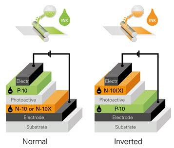
Figure 1. OPV Cell-regular (normal) and inverted architectures
WO3?nanoparticle inks can be used as HEL materials in OPV batteries due to their high functionality, excellent processability, and the ability to form layers on both hydrophilic and hydrophobic substrates.ZnO and AZO nanoparticle inks have similar advantages as EEL materials. All these inks can be applied to both conventional and inverted OPV cells. Top scientists have tested the performance of these inks as hole- and electron-selective interface layers in OPV batteries. The results show that the performance of these inks is similar to, if not better than, state-of-the-art materials such as PEDOT:PSS, and that they are perfectly suited for use in full solution-processed modules.1,2
ADVANTAGES OF INORGANIC INTERFACE LAYER INKS
The main advantages of the interface layer inks are:
● Suitable for various coating techniques such as slot-dye, doctor blading, and spin-coating
●?Requires low annealing temperatures (below 100°C) for layer formation
● Exhibits excellent wettability, even on hydrophobic substrates like the surface of the photoactive layer
● Boasts an extended shelf life
● Ensures high batch-to-batch reproducibility, with narrow specification ranges in viscosity, wettability, and particle size
● Does not contain aggressive or harsh chemicals, allowing deposition on organic photoactive materials without causing damage
● Resistant to degradation due to its inorganic nature
● Tungsten oxide nanoparticle ink can be seamlessly blended with PEDOT:PSS formulations for precise tuning of electronic and morphological properties in the resulting dry layer, such as conductivity, surface roughness, or layer porosity.
Reference
1.?Stubhan T, Li N, Luechinger NA, Halim SC, Matt GJ, Brabec CJ. 2012. High Fill Factor Polymer Solar Cells Incorporating a Low Temperature Solution Processed WO3Hole Extraction Layer. Adv. Energy Mater.. 2(12):1433-1438. https://doi.org/10.1002/aenm.201200330
2.?Li N, Stubhan T, Luechinger NA, Halim SC, Matt GJ, Ameri T, Brabec CJ. 2012. Inverted structure organic photovoltaic devices employing a low temperature solution processed WO3 anode buffer layer. Organic Electronics. 13(11):2479-2484. https://doi.org/10.1016/j.orgel.2012.06.045


 危险品化学品经营许可证(带存储)