 首页
首页 400-620-6333
Semiconductor Materials: A Summary of Questions
What is the band theory of semiconductors?
Valence band theory was proposed during the quantum revolution. Walter Heitler and Fritz London discovered the band.
We know that electrons in atoms exist in different energy levels. When we try to assemble a solid lattice with N atoms, then each layer of atoms must break down into N layers in the solid. The splitting of these sharp, tightly packed energy levels forms energy bands. The gap between adjacent bands representing a set of energies that do not contain electrons is called a band gap.

Figure 1: Band diagram of semiconductors, conductors and insulators
Valence Band
A band containing the energy levels of a valence electron is called a valence band. It's the highest energy band. Semiconductors have a smaller band gap than insulators. It al- lows electrons in the valence band to jump into the conduction band if they receive any external energy.
Conduction Band
It is the lowest unoccupied band containing either positive (hole) or negative (free electron) carrier energy levels. It has electrons that conduct electricity, causing it to flow. The conduction band has a higher energy level and is general y an air conduction band. A conduction band in a semiconductor can accept valence band electrons.
What are the properties of semiconductor materials?
Semiconductors can conduct electricity under good conditions or circumstances. Semiconductors also make excellent materials because they can conduct electricity on demand in a controlled manner.
Unlike conductors, charge carriers in semiconductors are created only because of external energy (thermal agitation). It causes a certain number of valence electrons to jump across the energy gap and into the conduction band, leaving an equal number of unoccupied energy states, known as holes. Conduction caused by electrons and holes is also important.
üConductivity: 105?~ 10-6?mho/m
üTemperature Coefficient of Resistance: negative
üCurrent Flow Way: electrons and holes
What is the Fermi level of a semiconductor?
There are Fermi levels between the valence and conduction bands (with Ef?Denotes). It's the highest molecular orbital that's occupied at absolute zero. Carriers in this state have their own quantum states and do not normally interact. At temperatures above absolute zero, these carriers will begin to occupy states above the Fermi level.
In a P-type semiconductor, the density of the unfilled states increases. So you can hold more electrons in lower energy states. In N-type semiconductors, however, the ?density of states increases and, as a result, more electrons are accommodated at higher energy levels.
Why does the resistivity of the semiconductor decrease with increasing temperature?
The difference in resistivity between conductors and semiconductors is due to the?difference in their carrier densities. The resistivity of the semiconductor decreases with increasing temperature because the number of carriers increases rapidly with increasing temperature, making the fractional change i.e., the temperature coefficient negative.
Common semiconductor types
Semiconductors can be divided into:
Intrinsic Semiconductor Intrinsic Semiconductor
Extrinsic Semiconductor (insic Semiconductor)
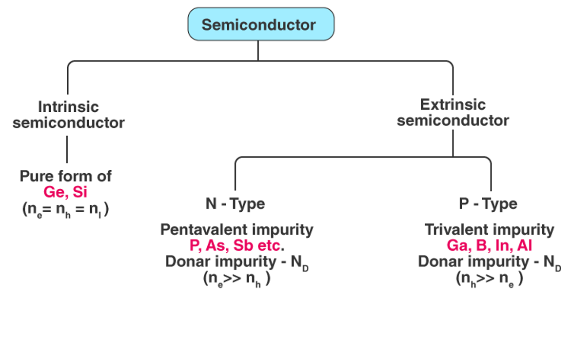
Figure 2: Semiconductor classification diagram
Intrinsic semiconductor
A pure semiconductor that is completely free of impurities and has no lattice defects is called an intrinsic semiconductor, which consists of only one type of element.
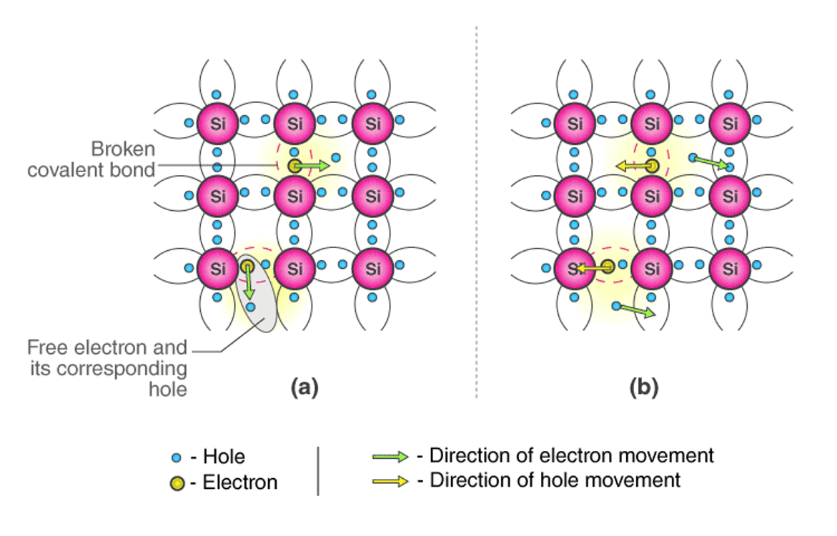
Figure 3: Diagram of the conduction mechanism of an intrinsic semiconductor: (a) with no electric field and (b) with an electric field
Germanium (Ge) and silicon (Si) are the most common types of intrinsic semiconductor elements. They have four valence electrons. They are covalently bonded to atoms at absolute zero degrees.
When the temperature is raised, most of the electrons break free due to collisions and move freely in the lattice, resulting in the absence of electrons in their original positions (holes). These free electrons and holes help conduct electricity in the semiconductor. The negative and positive charges have the same number of carriers.

Figure 4: Intrinsic semiconductor band diagram
Non intrinsic semiconductor
The conductivity of a semiconductor can be greatly improved by introducing a small number of replacement atoms. The process of adding alternative atoms to a pure semiconductor is called doping. Usually, at 107Only one of the atoms is replaced by a doped atom in a doped semiconductor. Non-intrinsic semiconductors can be further classified as N-type semiconductors and P-type semiconductors.
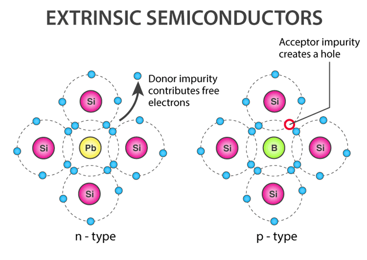
Figure 5: Classification of non-intrinsic semiconductors
N type semiconductor
?The electron is the main carrier
??I= Ih?and nh> > ne
When a pure semiconductor (silicon or germanium) is doped with a pentavalent impurity (P, As, Sb, Bi), four of the five valence electrons bond with four of Ge or Si's electrons. The fifth electron of the dopant is released. Thus, the impurity atom provides a free electron for conduction in the lattice. Since the number of free electrons increases with the addition of impurities, negative charge carriers also increase. Therefore, it is called N-type semiconductor.
The crystal as a whole is neutral, but the donor atom becomes a non-moving positive ion. Since conduction is due to a large number of free electrons, the electrons in N-type semiconductors occupy the majority of charge carriers and the holes are the minor it y carriers.
P type semiconductor
? The hole is the main carrier
? I = Ih?and nh> > ne
When a pure semiconductor is doped with a trivalent impurity (B, Al, In, Ga), three of the impurity's valence electrons bond to three of the semiconductor's four valence electrons. This leaves a lack of electrons (holes) in the impurities. These impurity atoms ready to receive bonding electrons are called "acceptors".
As the number of impurities increases, so do the holes (positive charge carriers). Therefore, it is called P-type semiconductor. The crystal as a whole is neutral, but the acceptor becomes a negative ion that does not move. Since the conduction is due to a large number of holes, the holes in P-type semiconductors are the majority of charge carriers, and the electrons are the minority of charge carriers.
Why is the valence band of a semiconductor partially filled at room temperature?
For a semiconductor, at absolute zero the conduction band is empty and the valence?
band is completely filled. At this temperature, valence band electrons cannot cross the conduction band. But at room temperature, as long as the band gap is small enough ?(such as 1ev), some electrons in ?the ?valence ?band ?can jump to the ?conduction band, so that the conduction band also gradual y fills with electrons.

 危险品化学品经营许可证(带存储)